- 您现在的位置:买卖IC网 > Sheet目录3841 > PIC24FJ128GA008-I/PT (Microchip Technology)IC PIC MCU FLASH 128K 80TQFP
2005-2012 Microchip Technology Inc.
DS39747F-page 121
PIC24FJ128GA010 FAMILY
14.0
OUTPUT COMPARE
14.1
MODES OF OPERATION
Each output compare module has the following modes
of operation:
Single Compare Match mode
Dual Compare Match mode generating:
- Single Output Pulse mode
- Continuous Output Pulse mode
Simple Pulse-Width Modulation mode:
- with Fault protection input
- without Fault protection input
14.2
Setup for Single Output Pulse
Generation
When the OCM control bits (OCxCON<2:0>) are set to
‘100’, the selected output compare channel initializes
the OCx pin to the low state and generates a single
output pulse.
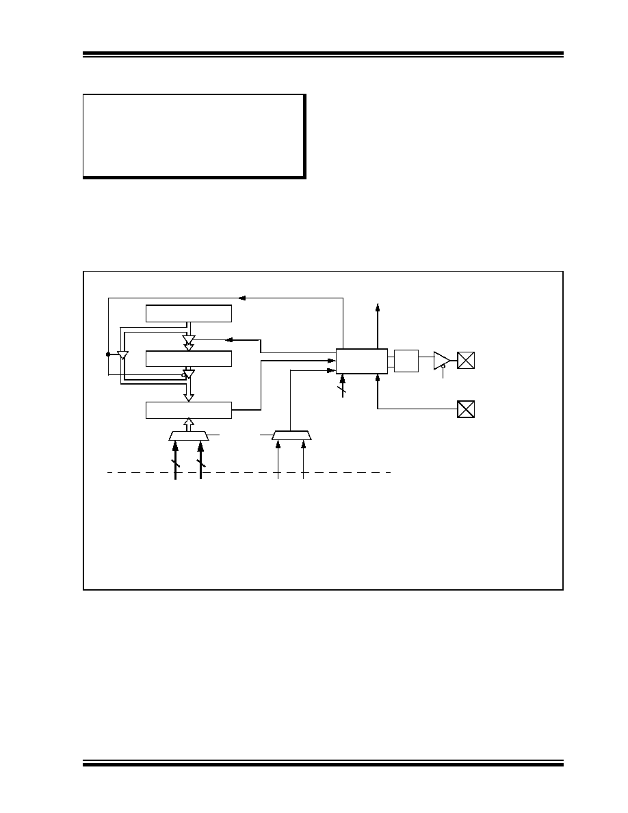
FIGURE 14-1:
OUTPUT COMPARE MODULE BLOCK DIAGRAM
Note:
This data sheet summarizes the features of
this group of PIC24F devices. It is not
intended to be a comprehensive reference
source. Refer to Section 16. “Output
Compare”
(DS39706) in the “PIC24F
Family
Reference
Manual”
for more
information.
Comparator
Output
Logic
Q
S
R
OCM<2:0>
Output Enable
OCx(1)
Set Flag bit
OCxIF(1)
OCxRS(1)
Mode Select
3
Note 1:
Where ‘x’ is shown, reference is made to the registers associated with the respective output compare channels, 1
through 5.
2:
OCFA pin controls OC1-OC4 channels; OCFB pin controls OC5.
3:
Each output compare channel can use either Timer2 or Timer3.
OCTSEL
0
1
16
OCFA or OCFB(2)
TMR Register Inputs
from Time Bases
(see Note 3)
Period Match Signals
from Time Bases
(see Note 3)
0
1
OCxR(1)
发布紧急采购,3分钟左右您将得到回复。
相关PDF资料
PIC16F737-I/SP
IC PIC MCU FLASH 4KX14 28DIP
PIC18F86K22-I/PTRSL
MCU PIC 64K FLASH XLP 80TQFP
PIC16C63A-04I/SP
IC MCU OTP 4KX14 PWM 28DIP
PIC16C63A-04I/SO
IC MCU OTP 4KX14 PWM 28SOIC
52559-2270
CONN FFC 22POS .5MM VERT ZIF SMD
52559-1870
CONN FFC 18POS .5MM VERT ZIF SMD
DSPIC33EP64MC506-I/PT
IC DSC 16BIT 64KB FLASH 64TQFP
52745-1896
CONN FFC 18POS .5MM R/A ZIF SMD
相关代理商/技术参数
PIC24FJ128GA008T-I/PF
制造商:MICROCHIP 制造商全称:Microchip Technology 功能描述:64/80/100-Pin General Purpose, 16-Bit Flash Microcontrollers
PIC24FJ128GA008T-I/PT
功能描述:16位微控制器 - MCU 128KB 69I/O RoHS:否 制造商:Texas Instruments 核心:RISC 处理器系列:MSP430FR572x 数据总线宽度:16 bit 最大时钟频率:24 MHz 程序存储器大小:8 KB 数据 RAM 大小:1 KB 片上 ADC:Yes 工作电源电压:2 V to 3.6 V 工作温度范围:- 40 C to + 85 C 封装 / 箱体:VQFN-40 安装风格:SMD/SMT
PIC24FJ128GA010
制造商:MICROCHIP 制造商全称:Microchip Technology 功能描述:General Purpose, 16-Bit Flash Microcontrollers
PIC24FJ128GA010_09
制造商:MICROCHIP 制造商全称:Microchip Technology 功能描述:64/80/100-Pin General Purpose, 16-Bit Flash Microcontrollers
PIC24FJ128GA010_12
制造商:MICROCHIP 制造商全称:Microchip Technology 功能描述:64/80/100-Pin, General Purpose, 16-Bit Flash Microcontrollers
PIC24FJ128GA010-I/PF
功能描述:16位微控制器 - MCU 16 Bit 128KB Flash 8Kb RAM 53 I/O RoHS:否 制造商:Texas Instruments 核心:RISC 处理器系列:MSP430FR572x 数据总线宽度:16 bit 最大时钟频率:24 MHz 程序存储器大小:8 KB 数据 RAM 大小:1 KB 片上 ADC:Yes 工作电源电压:2 V to 3.6 V 工作温度范围:- 40 C to + 85 C 封装 / 箱体:VQFN-40 安装风格:SMD/SMT
PIC24FJ128GA010-I/PT
功能描述:16位微控制器 - MCU 128KB 84 I/O RoHS:否 制造商:Texas Instruments 核心:RISC 处理器系列:MSP430FR572x 数据总线宽度:16 bit 最大时钟频率:24 MHz 程序存储器大小:8 KB 数据 RAM 大小:1 KB 片上 ADC:Yes 工作电源电压:2 V to 3.6 V 工作温度范围:- 40 C to + 85 C 封装 / 箱体:VQFN-40 安装风格:SMD/SMT
PIC24FJ128GA010T-I/PF
制造商:MICROCHIP 制造商全称:Microchip Technology 功能描述:64/80/100-Pin General Purpose, 16-Bit Flash Microcontrollers